Your degree is not enough for VLSI jobs. Learn real tools, real workflows, and become industry-ready.
The semiconductor industry is paying ₹18–26 LPA for VLSI engineers (freshers) and actively hiring from electronics backgrounds.
This IIT Bhubaneswar PG Diploma gives you the credential and the skills to make that move in 12 months.
IIT Bhubaneswar Certified
4-Week On-Campus
Minimum 7.5 LPA CTC
NIRF Ranked #22
IIT PG Diploma in VLSI with Placement Support Up to 18 LPA+
Your degree is not enough for VLSI jobs. Learn real tools, real workflows, and become industry-ready.
The semiconductor industry is paying ₹18–26 LPA for VLSI engineers (freshsers) and actively hiring from electronics backgrounds.
This IIT Bhubaneswar PG Diploma gives you the credential and the skills to make that move in 12 months.
IIT Bhubaneswar Certified
4-Week On-Campus
Minimum 7.5 LPA CTC
NIRF Ranked #22
India’s #1st IIT + Industry Collaborated Program
IIT Bhubaneswar's
Post Graduate Diploma Program
Build a high-growth career in VLSI & Semiconductor Technology with India’s most industry-focused postgraduate diploma. Learn from IIT faculty and top industry leaders with 20+ years of experience at Micron, Samsung, and ams OSRAM.
Earn Alumni Status from IIT
Globally Valued VLSI Diploma
Minimum 7.5 LPA CTC
Build highly qualified network
Ranked #22
India’s #1st IIT + Industry Collaborated Program
IIT Bhubaneswar's
Post Graduate Diploma Program
Build a high-growth career in VLSI & Semiconductor Technology with India’s most industry-focused postgraduate diploma. Learn from IIT faculty and top industry leaders with 20+ years of experience at Micron, Samsung, and ams OSRAM.
Earn Alumni Status from IIT
Globally Valued VLSI Diploma
Minimum 7.5 LPA CTC
Build highly qualified network
Ranked #22
12 Months
11 Month Online + 4 Weeks on campus
INR 9,999/Month*
Easy EMI from
Upto 18 LPA
Min 7.5LPA Guaranteed CTC*
100%
Placement Support
Backed by Real Numbers, Driven by Industry Growth
Program Advantages
This PG Diploma in Semiconductor Technology & Chip Design is uniquely designed to combine the academic prestige of IIT Bhubaneswar with the real-world expertise of MOSart Labs, giving you job-ready skills, global credibility, and career acceleration in the fast-growing semiconductor industry.
$160 Billion Market by 2030
India’s semiconductor market stood at USD 38–53 billion in 2024 and is set to grow to USD 100–160 billion by 2030, expanding at 12–18% CAGR.
1.2 Million Workforce Vision
The Indian government is actively building a pipeline of 1.2 million professionals, including 275,000 chip designers by 2032.
Up to ₹80 Lakhs/Year
Earn up to ₹80 lakhs annually (~USD 93,000). Even freshers in VLSI start with packages significantly higher than average electronics graduates.
Upto 24 LPA
MOSart Labs provides placement support and Helps you land a job of min ₹7.5 LPA CTC, a safety net that very few programs offers.
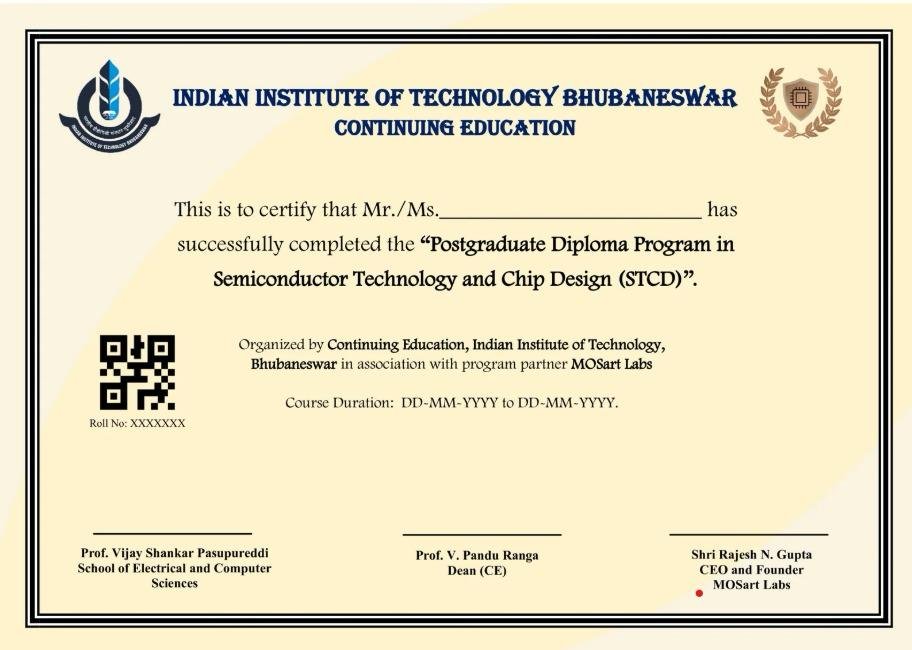
IIT-Certified Diploma
Earn a Professional Diploma jointly awarded by IIT Bhubaneswar & MOSart Labs. 90% of employers value IIT-certified programs as a strong credential.
500+ Lab Hours
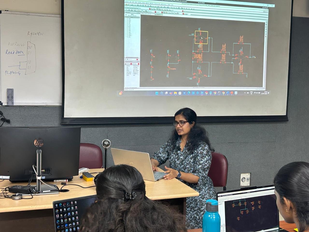
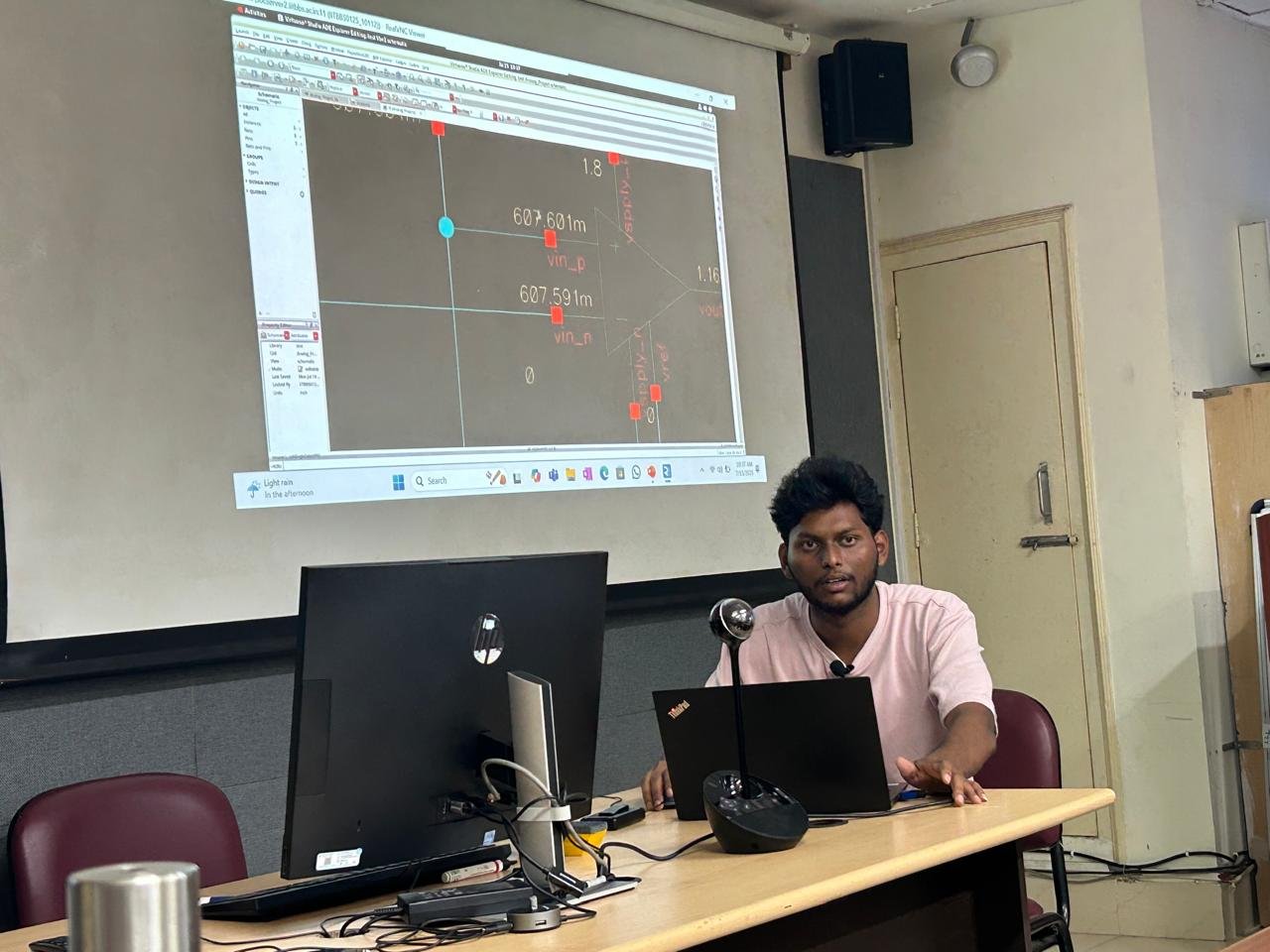
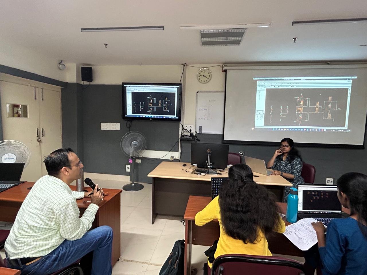
Practical labs using industry-grade EDA tools, you don’t just study concepts you master skills that employers test for in real-world design roles.
This is where most
ECE/EEE graduates get stuck.
❌
You have the degree. But companies expect real skills.
❌
You see others getting placed. You’re still trying to figure it out.
❌
You studied electronics. But you’re not sure what to do next.
❌
You don’t want another course that doesn’t lead to a real job.
This is exactly the gap most students face. And this is exactly what this program is built to solve.
It builds on your electronics foundation, adds real VLSI skills using industry tools, and prepares you for actual chip design roles.
This is where most
ECE/EEE graduates get stuck.
❌
You have a degree. But companies expect real skills.
❌
You see others getting placed. You’re still trying to figure it out.
❌
You studied electronics. But you’re not sure what to do next.
❌
You don’t want another course that doesn’t lead to a real job.
This is exactly the gap most students face. And this is exactly what this program is built to solve
This is exactly the gap most students face. And this is exactly what this program is built to solve
Our PG Diploma in Semiconductor Technology & Chip Design blends strong fundamentals with cutting-edge specialization. The curriculum is designed in 6 Phases, ensuring you graduate industry-ready.
Phase 1
Launch Pad Training & Exam
Build core semiconductor fundamentals and get IIT-ready. Qualify for the Foundation Semester through assessments.
Phase 2
Foundation Semester
Learn 5 core VLSI subjects with hands-on projects. Strengthen fundamentals for advanced specialization.
Phase 3
2-Week Campus Immersion
Experience learning at IIT with faculty and lab exposure. Gain industry insights and advanced technical knowledge.
Phase 4
Specialization Semester
Choose Digital, Analog, Verification, Layout or Physical Design. Complete 3 projects + 1 capstone aligned to industry tools.
Phase 5
2-Week Campus Immersion
Advanced training at IIT with mentorship and networking. Prepare for high-impact semiconductor careers.
Phase 6
Placement & Job Support
Placement training with hiring drives from top Semiconductor companies. Job opportunities up to 18* LPA.
Who will you learn from?
Meet Our Faculty
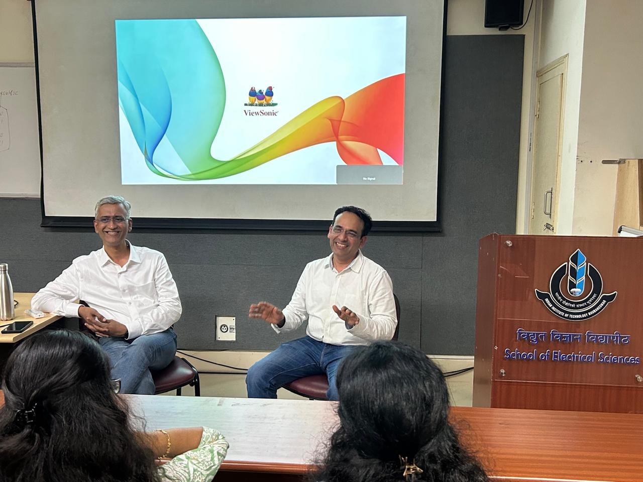
Not professors. Engineers who’ve shipped real silicon with 25+ years of VLSI expertise.