Uncategorized
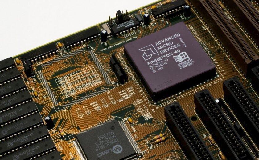
India is no longer just a consumer of electronics—it’s emerging as a semiconductor powerhouse. Fueled by strategic investments, policy reforms, and skill development initiatives, a robust ecosystem is taking shape. For VLSI engineers and design specialists, this translates into unprecedented career opportunities and growth.
Let’s explore the key government initiatives making it happen—and how you can position yourself to benefit.
1. Semicon India Programme (₹76,000 crore)
Launched in 2021, this flagship initiative offers 50% capital subsidy for fabs, display fabs, compound semiconductors, and packaging/assembly/testing (ATMP/OSAT) units. A Design Linked Incentive (DLI) provides up to 50% subsidy on chip design infrastructure and 4–6% on product sales.
Impact: 5 projects approved so far—covering Micron, Tata, Kaynes, and CG Power—with production capacities in millions per day
2. SPECS & PLI Schemes
- SPECS offers 25% capex incentive on manufacturing of electronic components, micro/nano components, semiconductors, and solar PV components
- PLI for Large-Scale Electronics gives 3–6% incentive on incremental sales for mobile and components manufacturing, catalyzing ₹8,390 crore investment & ₹5 lakh crore production until mid-2024 .
Together, these schemes nurture the design-to-manufacture pipeline, opening up roles in semiconductor product development and backend fabrication.
3. Skill Development & Academic Reform
- AICTE introduced B.Tech programs in Electronics (VLSI Design & Technology) and diplomas in IC manufacturing
- The Chips to Startup (C2S) initiative will train ~85,000 engineers in VLSI and embed design, targeting 175 ASICs, 20 SoCs, 30 FPGA designs by 2027 across 120+ institutions
- IIT Kanpur, Madras and others are adding semiconductor hardware, fabrication, and packaging modules to their curriculum
- Apprenticeships under ESSC & NAPS have scaled from ~7.5K to ~92K in 2023‑24
Outcome: Closing the gap—India needs ~275K chip‑design, ~25K fab, and ~29K ATMP professionals by 2032
4. Manufacturing Push: Fabs, OSAT, Clusters
- Tata TSAT is building India’s first green-field OSAT in Assam—a ₹27,000 crore project creating up to 30,000 jobs
- States are rolling out supportive policies: Uttar Pradesh’s Semiconductor Policy has attracted ₹40,000 crore in proposals
These facilities generate massive demand for VLSI talent—for design, validation, and backend roles.
5. Industry–Academia Collaboration
Global companies like AMD, Micron, LAM Research, Synopsys are conducting boot camps, faculty training, campuses, and mentorship programs
- AMD offers design-focused apprenticeships involving its CPU/GPU teams.
- LAM and IISc partnership aims to upskill 60,000 engineers via “Semiverse”
- Synopsys SARA works with IITs to develop standardized curricula
This ensures students not only earn degrees, but also get hands-on EDA tool experience.
Career Impact for VLSI Engineers
- Design & Verification roles surge as fabs and OSAT units start operations.
- Academia-backed VLSI programs translate directly to core VLSI jobs in front-end/back-end teams.
- Government push brings global chip companies to India—creating high-paying, large-scale hiring.
- Established collaboration ensures exposure to EDA tools, chip flows, applied research—key differentiators in hiring.
How MOSart Labs Helps You Leverage This Boom
As government-backed investments spearhead India’s semiconductor ambition, the demand for job-ready VLSI talent is skyrocketing. At MOSart Labs, we offer:
- An IIT-certified VLSI PG Diploma aligned with India’s curriculum changes.
- Hands-on experience across RTL, verification, STA, PD, DFT, using Synopsys, Cadence, Mentor tools.
- Industry-grade projects in ASIC, FPGA, SoC—exactly the profiles employers are hiring for.
- Placement support targeted at emerging fab, test, OSAT, and design hubs.
Final Thoughts
India’s quest for semiconductor sovereignty—backed by massive investments, policy reforms, and academic initiatives—is opening unmatched opportunities for VLSI engineers. Whether you’re seeking design roles, fab-based careers, or test and packaging jobs, now is the time to get VLSI-ready.
Join MOSart Labs to align your skills with India’s semiconductor future—and build a secure, high-growth career in the heart of the action.