Ranked #1 on Chip Design
From Chip-to-Product. From Classroom-to-Career.
Master Analog & Digital IC Design with industry-grade projects, 100% placement support, and training by semiconductor leaders.
Admission Closing Soon in
Few Seats Left
(6M Class + 4M Internship)
Easy EMI from
of Hands-On Labs
Placement Support
Why This Program Stands Out
This program gives you a real competitive advantage by combining industry recognition, practical project work, and expert mentorship to ensure you gain job-ready skills, stand out to employers, and accelerate your career in IC design.
Massive demand for skilled IC designers worldwide.
High salary potential right from the start of your career.
Huge opportunity in market with a 45% CAGR growth rate.
Recognized by an active chip design company, not just a training institute.
4-month internship with real project experience and certification.
End-to-end chip design projects that mirror real industry challenges.
This program blends 6 months of structured training with a 4-month internship, preparing you to work as a real VLSI engineer. You’ll start with strong foundations in Analog and Digital IC Design, move into advanced specialization, and finally execute a complete chip design project from specification to verification inside an active semiconductor company environment.
Foundation
Mini Corporate Project
Specialization Module
Internship & Capstone Project
Apply your foundation knowledge to real-world problems by choosing a specialization (Analog or Digital) and working on industry-oriented challenges.
Execute a complete full-cycle chip design project in a real industry environment:
Begin by understanding the problem statement and design requirements. Define clear specifications for power, performance, area, and cost, just like engineers do in top MNCs.
Translate specifications into a structured system architecture. Break down the chip into functional blocks and plan signal flow, interfaces, and dependencies.
Move from theory to execution by building detailed schematics. Use industry-grade tools to simulate circuit behavior, ensuring that designs meet performance targets.
Bring all modules together into a complete system. Conduct integration testing to ensure smooth interaction between blocks and verify overall chip functionality.
Run rigorous verification processes to confirm design accuracy. Test for real-world conditions like process variation, temperature, and noise, ensuring robust performance and high yield.
Present your project in a capstone defense to industry experts. Showcase your methodology, design choices, and test results, preparing you for real-world reviews and technical interviews.
MOSart Semi is a new-generation IC design and product engineering company, built by semiconductor industry veterans with over five decades of combined experience at Micron, Texas Instruments, ams OSRAM, TRAM Semiconductors, and other global leaders.
Unlike traditional training institutes, MOSart Labs is an active chip design company delivering real projects to global clients such as Dell, Apple, Samsung, and Tesla. This gives our students a unique edge — they learn in the same environment where world-class chips are being designed.
Who will you learn from?
Our founders, with 25+ years of VLSI expertise, are also your trainers.
Founder & CEO
With over 27 years of experience in the VLSI industry, Rajesh has led semiconductor innovations at TRAM Semiconductors, Texas Instruments, and Micron. At MOSart Labs, he drives the mission of transforming engineers into industry-ready chip designers.
Founder & CTO
Bringing 23 years of expertise in VLSI design, Krishna has worked with global semiconductor leaders including ams OSRAM. His vision is to bridge the gap between academic learning and real-world chip design practices through hands-on training and advanced R&D.
VP R & D
with 25 years in the VLSI industry and former Director at Samsung, is an NIT Trichy alumnus. He specializes in SoC architecture, CPU/GPU/NPU development, and has collaborated with global leaders including Apple, Dell, Micron, and Toshiba.
By the end of this program, you won’t just know the theory you’ll have industry-grade project experience that proves your skills.
Work on a full-cycle IC design project from specification to silicon.Deliver corporate-level mini projects and defend your capstone project in front of industry experts.
Graduate with a project portfolio that showcases your ability to contribute from Day 1 in an MNC.
Analog Design engineer
Digital Design engineer
Analog Circuit Design Engineer
Digital Circuit Design Engineer
Connect with our program advisor and get all your queries answered.
The program includes 6 months of intensive coursework followed by a 4-month industry internship in an IP design project.
Final-year students and graduates from Electronics, VLSI, Communication, Instrumentation, or Physics backgrounds are eligible to apply.
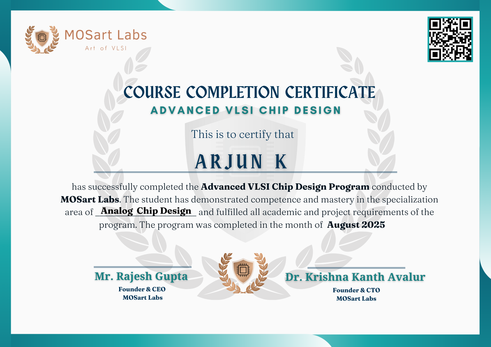
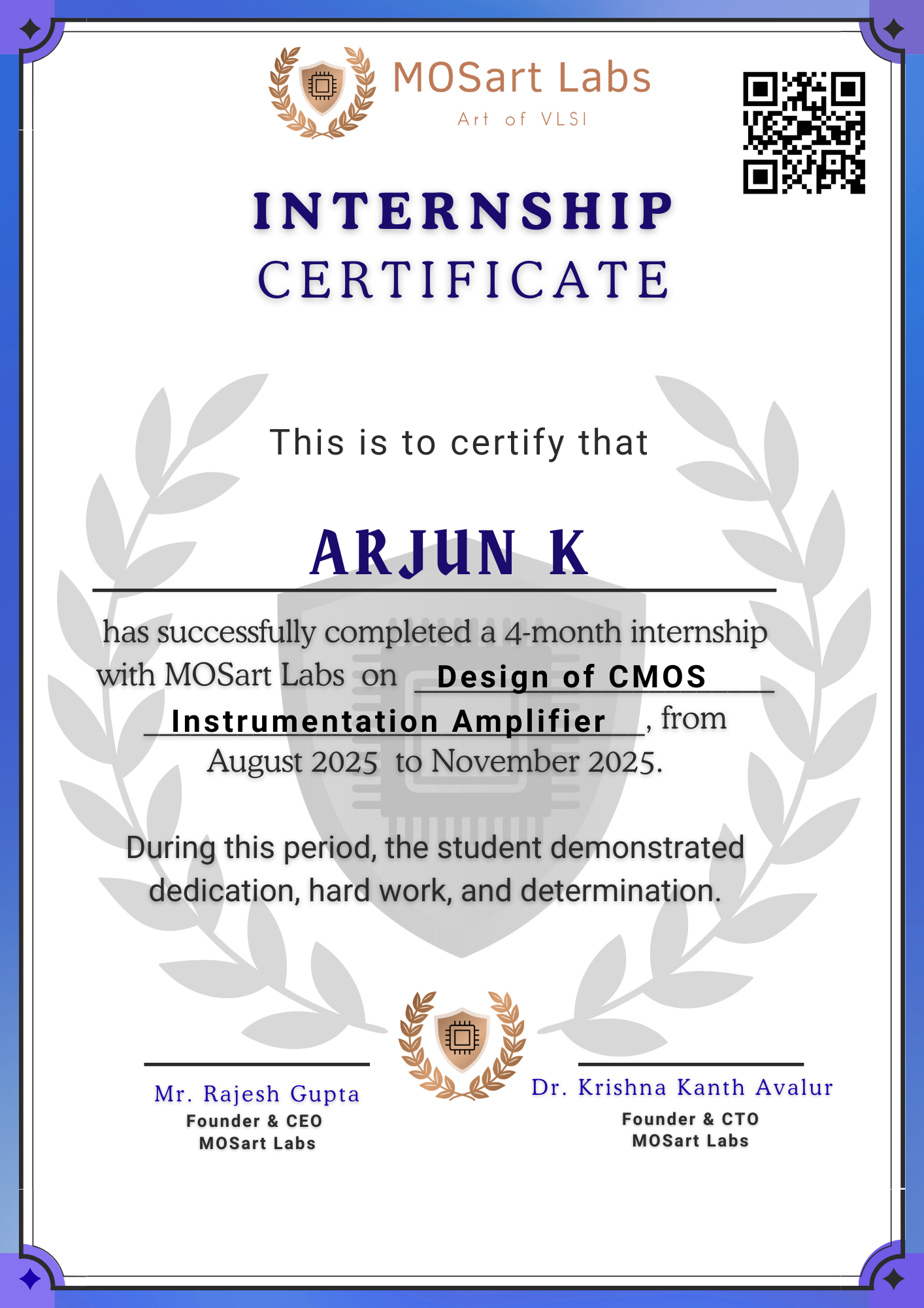
You will receive a Course Completion Certificate and an Internship Certificate directly from Mosart Labs, a recognized chip design company.
Yes. Mosart Labs provides 100% placement support, along with career guidance and interview preparation, to help you connect with semiconductor companies until you are successfully placed.
We offer flexible EMI options starting at ₹6,250/month and limited-time scholarships to make the program affordable.
You’ll work on mini, corporate, and capstone projects covering the entire chip design cycle – from specification to silicon to system.
The program is fully online with 24/7 remote access to all industry-standard tools, so you can learn and practice from anywhere at any time.
Understand Your Investment
Invest in your future with flexible options designed to make learning accessible.
Limited-Time Scholarships Available. Block your seat with a minimal booking amount and secure exclusive discounts.
Have questions? Want to know if this program is the right fit for you?
Fill out the form and our team will get in touch with you.


