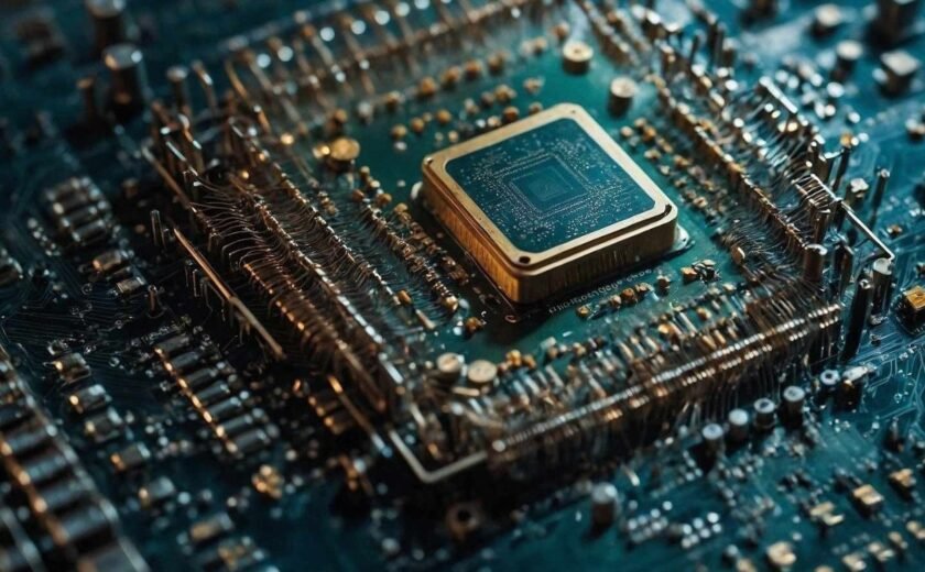
As integrated circuits grow more complex and shrink in size, ensuring they work perfectly becomes increasingly challenging. That’s where DFT (Design for Testability) comes in—a critical specialization in VLSI design that ensures chips can be tested efficiently before reaching customers.
Today, DFT engineers are in high demand across top semiconductor companies like Intel, AMD, Qualcomm, and TSMC, making this one of the most promising VLSI career paths in 2024 and beyond.
In this blog, we’ll explain what DFT means, why it matters, the tools and techniques used, and how you can build a career in DFT engineering.
What is DFT in VLSI?
DFT (Design for Testability) refers to a set of design techniques that make it easier to test the functionality and integrity of a silicon chip after it’s manufactured.
Without DFT, testing millions (or billions) of logic gates inside an integrated circuit would be practically impossible.
Why is DFT Important in Chip Design?
Modern-day SoCs (System on Chips) are massive—with multiple cores, memory blocks, and analog-digital interfaces. Any defect, no matter how small, can render a chip useless.
DFT helps identify manufacturing faults like:
- Stuck-at faults
- Bridging faults
- Delay faults
- Open circuits
Key Benefits of DFT:
- Ensures chips are defect-free before shipment
- Reduces debugging and field failure rates
- mproves time-to-market for semiconductor products
- Enables automated test pattern generation (ATPG)
Common DFT Techniques
1. Scan Insertion
Converts flip-flops into scan cells to enable easy shifting of test data through scan chains.
2. Boundary Scan (JTAG)
Used for board-level testing and debugging using standardized access ports.
3. Built-In Self-Test (BIST)
The chip tests itself by generating and analyzing test patterns internally.
4. Memory BIST (MBIST)
Used to test embedded memory blocks within a chip.
5. ATPG (Automatic Test Pattern Generation)
Generates patterns to detect faults post-manufacturing.
DFT vs Other VLSI Domains
| Feature | DFT Engineer | RTL/Design Engineer | Verification Engineer |
|---|---|---|---|
| Focus Area | Test structures and coverage | Functional logic design | Functional correctness |
| Tools Used | DFT Compiler, TetraMAX, FastScan | Design Compiler, Genus | ModelSim, QuestaSim, UVM |
| Hiring Demand | High (2024–2025 trend) | High | High |
| Growth Potential | Excellent | Strong | Strong |
Career Scope of DFT Engineers
With global semiconductor manufacturing growing rapidly, DFT is now a core hiring area for:
- Product Companies (Intel, AMD, NXP, Apple)
- Semiconductor Foundries (TSMC, GlobalFoundries)
- Design Service Companies (Wipro, Tata Elxsi, Sankalp, MosChip)
Top Roles in DFT:
- DFT Engineer
- ATPG Engineer
- BIST Implementation Specialist
- Memory Test Design Engineer
- DFT STA Engineer
Average Starting Salary (India):
₹6–10 LPA for freshers with DFT project exposure
₹15–25 LPA for professionals with 3–5 years experience
How to Become a DFT Engineer
1. Learn Core VLSI Concepts
Understand digital design, logic gates, flip-flops, multiplexers, FSMs, and Verilog HDL.
2. Specialize in DFT Techniques
Master scan chains, BIST, ATPG, MBIST, and fault models.
3. Get Hands-On with Industry Tools
Get trained on Synopsys DFT Compiler, TetraMAX, and Tessent.
4. Work on Real DFT Projects
Build projects that simulate scan insertion, generate ATPG patterns, and analyze test coverage.
5. Get Certified by a Reputed Institute
An IIT-certified VLSI course with DFT modules significantly boosts your placement chances.
Why MOSart Labs is the Best Launchpad for Your DFT Career
At MOSart Labs, our IIT Bhubaneswar-certified VLSI PG Diploma gives you in-depth training in:
- RTL design, STA, synthesis
- Advanced DFT techniques and real-world project work
- Access to licensed EDA tools like Synopsys and Cadence
- Placement assistance in top semiconductor companies
Whether you’re a fresher or working professional, MOSart Labs equips you with the exact skills the industry is hiring for in DFT engineering.
Final Thoughts
As chips grow more complex, Design for Testability is no longer optional—it’s essential. And that makes DFT one of the most rewarding and future-proof careers in VLSI.
If you’re looking to specialize in a high-demand area with strong growth, international opportunities, and technical depth—DFT is the path to take.
Build your DFT career with industry tools, expert mentorship, and IIT-certified training—only at MOSart Labs.


