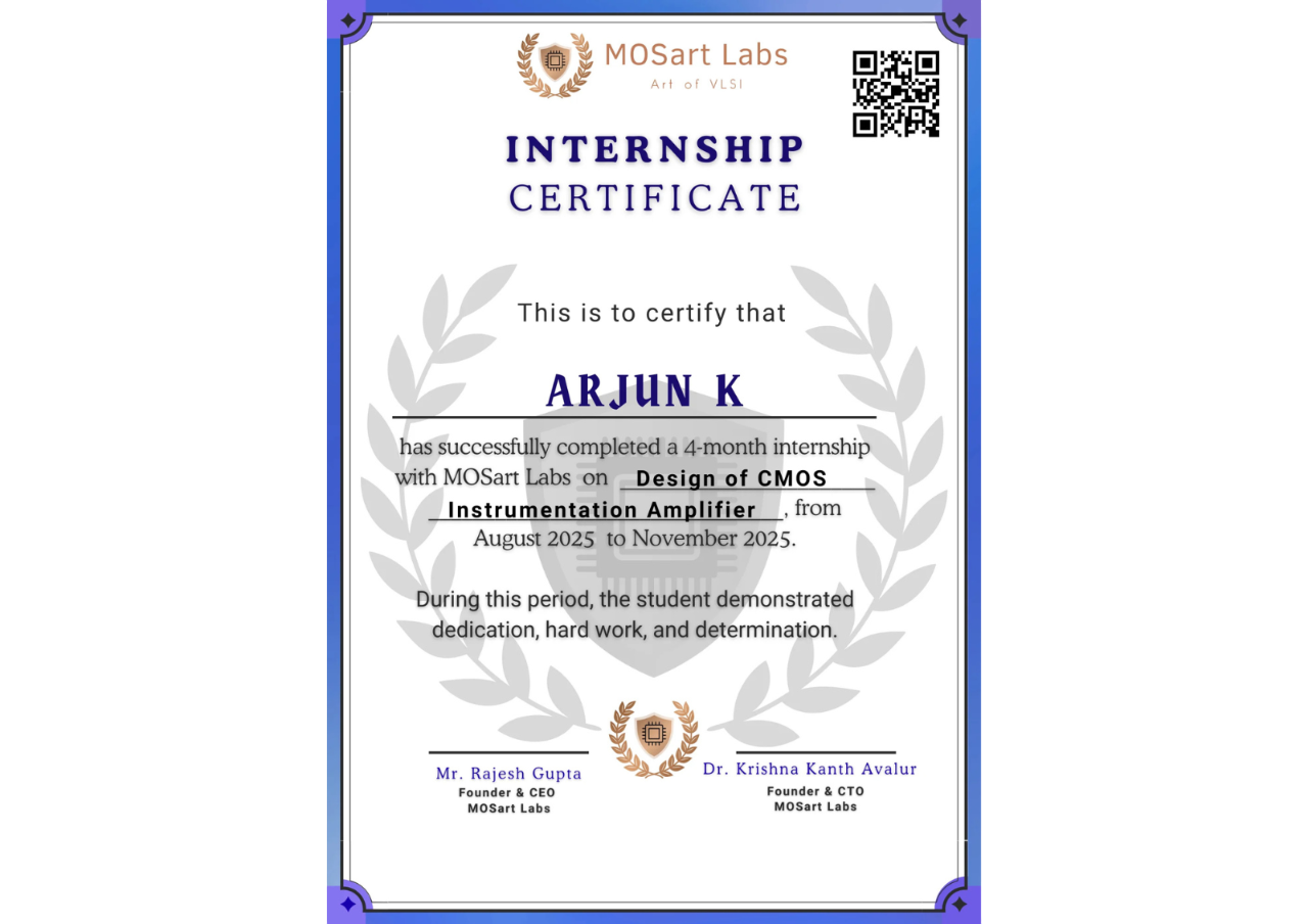
This program gives you a real competitive advantage by combining industry recognition, practical project work, and expert mentorship to ensure you gain job-ready skills, stand out to employers, and accelerate your career in IC design.
1.2M jobs by 2027
Massive demand for skilled IC designers worldwide.
₹6L – 18L Annually
High salary potential right from the start of your career.
₹4.2T Market by 2027
Huge opportunity in market with a 45% CAGR growth rate.
Industry-Endorsed Certification
Recognized by an active chip design company, not just a training institute.
Integrated Internship
4-month internship with real project experience and certification.
Hands-on Project Work
End-to-end chip design projects that mirror real industry challenges.
Choose from three specialized VLSI domains and build industry-ready skills through expert-led, industry-grade training. Our practical-first approach focuses on real-world projects, hands-on learning, and industry-standard tools—not just theory.
Advanced RTL Design
Master RTL Design using Verilog & SystemVerilog with hands-on training, real-world projects, and industry-standard EDA tools. Build synthesis-ready digital designs and become industry-ready.
Master Design Verification using SystemVerilog & UVM with hands-on training, real-world projects, and industry-standard EDA tools. Build robust testbenches and verify complex digital designs.
This program blends 6 months of structured training with a 4-month internship, preparing you to work as a real VLSI engineer. You’ll start with strong foundations in Analog and Digital IC Design, move into advanced specialization, and finally execute a complete chip design project from specification to verification inside an active semiconductor company environment.
Phase 1
3 Months (Foundation) with Course Project
Learn the core concepts of Analog & Digital Design. Build a strong technical base for advanced modules.
Phase 2
3 Months Specialization with Course Project
Choose your specialization: Analog or Digital. Work on a guided mini project. Apply concepts through practical hands-on tasks.
Phase 3
4 Months (Internship Project)
Work on an advanced industry-level internship project. Gain real semiconductor industry experience.
Phase 4
Internship Project Review
Get your internship project reviewed by industry experts. Build real-world semiconductor industry experience.
Phase 5
(Job Interview Preparation)
Build your portfolio and attend mock interviews. Prepare thoroughly for placement opportunities.
Phase 6
(Get Placed)
Attend interviews scheduled by our placement team. Crack your interviews and enter the semiconductor industry.
MOSart Semi is a new-generation IC design and product engineering company, built by semiconductor industry veterans with over five decades of combined experience at Micron, Texas Instruments, ams OSRAM, TRAM Semiconductors, and other global leaders.
Learn directly from VLSI experts with 25+ years of industry experience.
Get trained by professionals behind global semiconductor innovations.
Build exactly the skills top semiconductor companies demand.
Receive mentorship tailored to high-paying VLSI careers.
Train in a live chip design company, not just a classroom.
Unlike traditional training institutes, MOSart Labs is an active chip design company delivering real projects to global clients such as Dell, Apple, Samsung, and Tesla. This gives our students a unique edge — they learn in the same environment where world-class chips are being designed.
Check Eligibility
Who will you learn from?
Meet Our Leadership Team
Our founders, with 25+ years of VLSI expertise, are also your trainers.
The program includes 6 months of intensive coursework followed by a 4-month industry internship in an IP design project.
Who is eligible for this program?
Final-year students and graduates from Electronics, VLSI, Communication, Instrumentation, or Physics backgrounds are eligible to apply.
What kind of certificate will I receive?
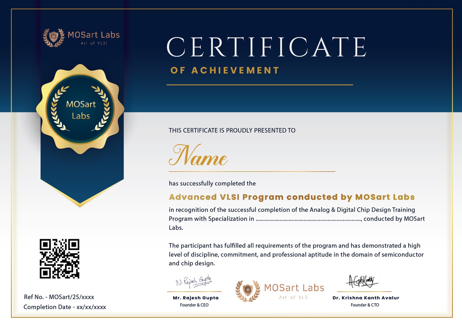
You will receive a Course Completion Certificate and an Internship Certificate directly from MOSart Labs, a recognized chip design company.
Do you provide placement support?
Yes. MOSart Labs provides 100% placement support, along with career guidance and interview preparation, to help you connect with semiconductor companies until you are successfully placed.
What are the payment options available?
We offer flexible EMI options starting at ₹6,250/month and limited-time scholarships to make the program affordable.
What kind of projects will I work on?
You’ll work on mini, corporate, and capstone projects covering the entire chip design cycle – from specification to silicon to system.
Is the program online or offline?
The program is fully online with 24/7 remote access to all industry-standard tools, so you can learn and practice from anywhere at any time.
Understand Your Investment
Program Fee & Scholarships
1,53,400 99,120 /-
Registration Fees
₹3,000/-
Pay Registration Fees to confirm and Secure you seat.
OneTime Payment
₹84,320/-
Opt for One – Shot Payment and save 11,800/-
OR
Part Payments
₹87,000/-
Pay in Parts: 21,750/ – per Installment for Four Months & save 9,120/-
OR
EMI/Loan Payment
₹96,120/-
Pay in Easy EMI’s Starting from 8,712/- Per Month
Easy EMI* Starts From ₹8,712/-
Registration fees cover the Launchpad training and exam.
Enroll Now is applicable only after clearing the Launchpad exam to block your seat.